


Design Hack: Why Via-in-Pad is the Secret to High-Density PCB Design
 View
View
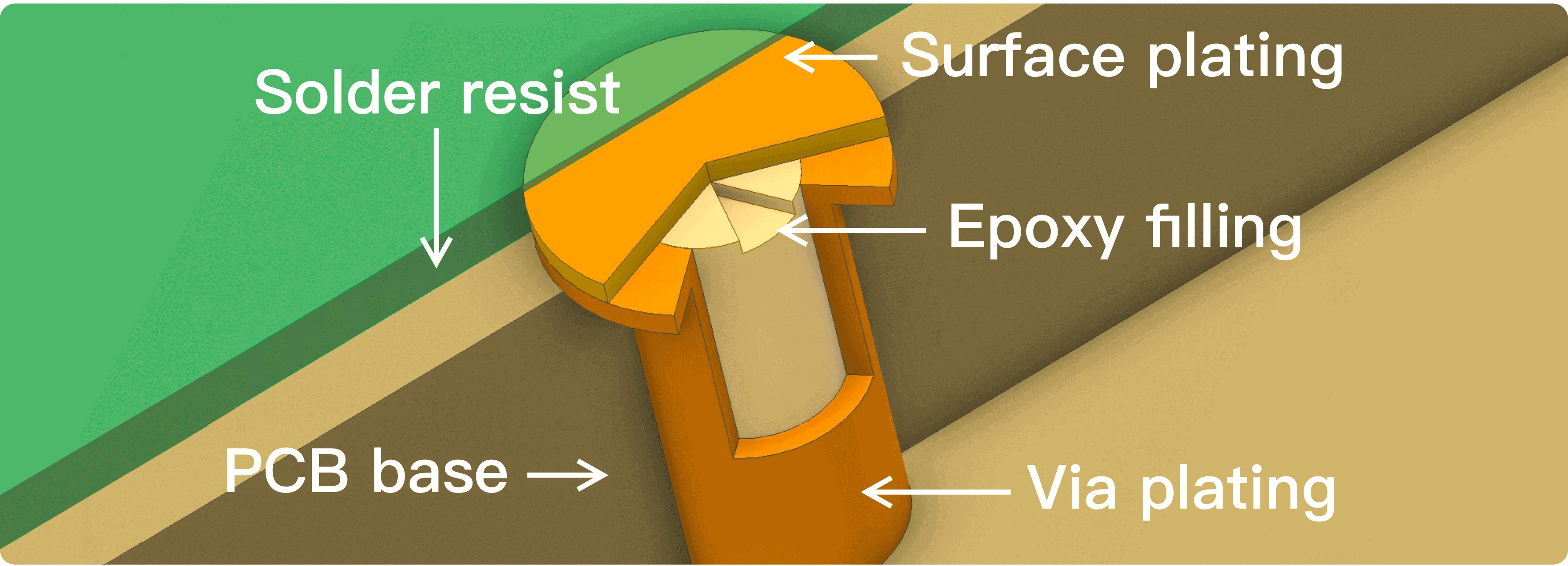
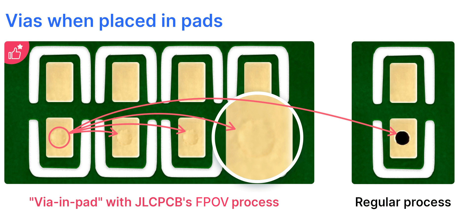
【What is Via-in-Pad (VIP)?】
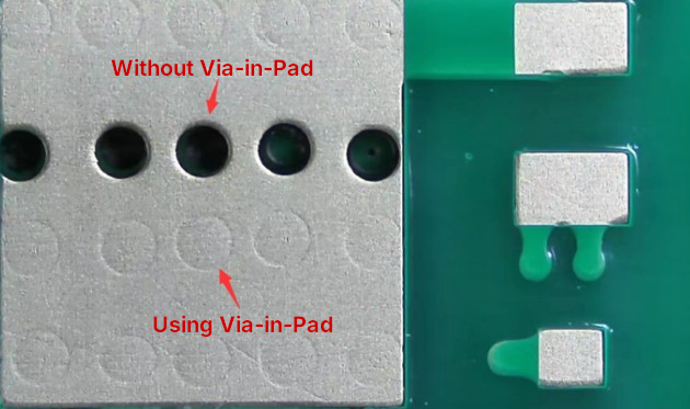
Traditionally, vias are placed away from component pads to avoid solder wicking. Via-in-Pad puts the via directly inside the SMD pad, plated and filled to create a flat, solderable surface.
【Why Use Via-in-Pad?】
- Space Saver: Essential for BGA components with tight pitches where there’s no room for traditional "dog-bone" fan-outs.
- Better Thermal Management: Vias directly under components help dissipate heat much more efficiently.
- Signal Integrity: Reduces inductance and path length, perfect for high-frequency designs.
【The Big News from JLCPCB】
Usually, Via-in-Pad is an "expensive" premium service because it requires extra POVE (Plating Over Via Filled with Epoxy) steps. But here’s the kicker: JLCPCB is now offering FREE Via-in-Pad (POVE) for multi-layer boards (6-20 layers) to help engineers push the boundaries of compact design without breaking the bank!
【Design Specs to Remember】
- Application: Best for BGAs and fine-pitch SMD components.
- Process: Epoxy filling + Copper capping (POVE) ensures no solder leakage and a perfectly flat pad.
- Eligibility: Check the 6+ layer board options during checkout to claim the $0 upgrade.
#PCBDesign #HardwareEngineering #JLCPCB #ViaInPad
 #PCBDesign#
#JLCPCB#
#PCBDesign#
#JLCPCB#
PCB
Sign In Or Register Comment after
No comments yet. Be the first to comment!